Introduction
Space Vector Pulse Width Modulation (SV-PWM) is a modulation scheme used to apply a given voltage vector to a three-phased electric motor (permanent magnet or induction machine).
The goal is to use a steady state DC-voltage and by the means of six switches (e.g. transistors) emulate a three-phased sinusoidal waveform where the frequency and amplitude is adjustable.
There are two challenges to this:
The only voltage level available is the DC-link voltage which can be assumed constant (well, at least for sake of simplicity).
There are only six different voltage angles available. With no middle ground. To rotate a motor, a smoothly rotating voltage vector is required - not one that skips 60 degrees per step.
grid supplied three phase voltage
A grid supplied three phase voltage will look like the animation below. This is what an induction machine is experiencing when connected directly to the grid.
The three phased system is illustrated using two different, but equal forms:
A vector diagram showing all three phases and their vector sum (space vector).
An ordinary instantaneous sine wave representation, also showing the resultant space vector.
An ordinary three phased system, here shown in both vector form and in sinusoidal form. The black vector is the resultant space vector; a vector sum obtained by adding the three vectors. As can be seen, the space vector's magnitude is always constant.
The topology of a two-level inverter
The two-level inverter is the most used topology today because it is simple and cheap. Higher level converters are mostly used for high voltage applications and will not be treated in this article.
The schematics of a two-level inverter with passive diode front-end, DC-link capacitor and a motor equivalent connected.
Snubbers and anti-parallel diodes are not shown.
The above schematic is the well-known and well-used inverter topology. From left to right the following is shown:
A three phase supply and a three-phased diode rectifier
A DC-link capacitor for energy storage and voltage stabilization
An inverter bridge with six transistors
Three output terminals and a star-connected (ungrounded) induction machine equivalent
Not shown: snubber circuit, anti-parallel diodes over the transistors and back-EMF in motor.
To better understand how space vector PWM is used, the above schematic can be greatly simplified:
First, the DC-link voltage can be simplified so that it is constant. Normally it varies with load, but not that much during the time frames given in this article. The supply and diode rectifier will thus not be shown for the rest of the article.
Second, each leg of the inverter bridge can be simplified by replacing the two bridge leg-transistors by one single SPDT-switch which shall indicate that either the top or the bottom transistor is closed. The scenario of both transistors in one leg being open is not interesting and will not be necessary. Further, the scenario of both transistors being closed implies that the DC-link is short circuited and we can all go home and order new parts.
The simplification from two transistors to one SPDT switch is possible because only one transistor in each bridge leg can be closed at any given time and that one transistor must be closed in each leg in order to have a three-phased current flowing. Additionally there are always anti-parallel diodes across each transistor to allow bi-directional current flow.
The simplified schematic is presented below:
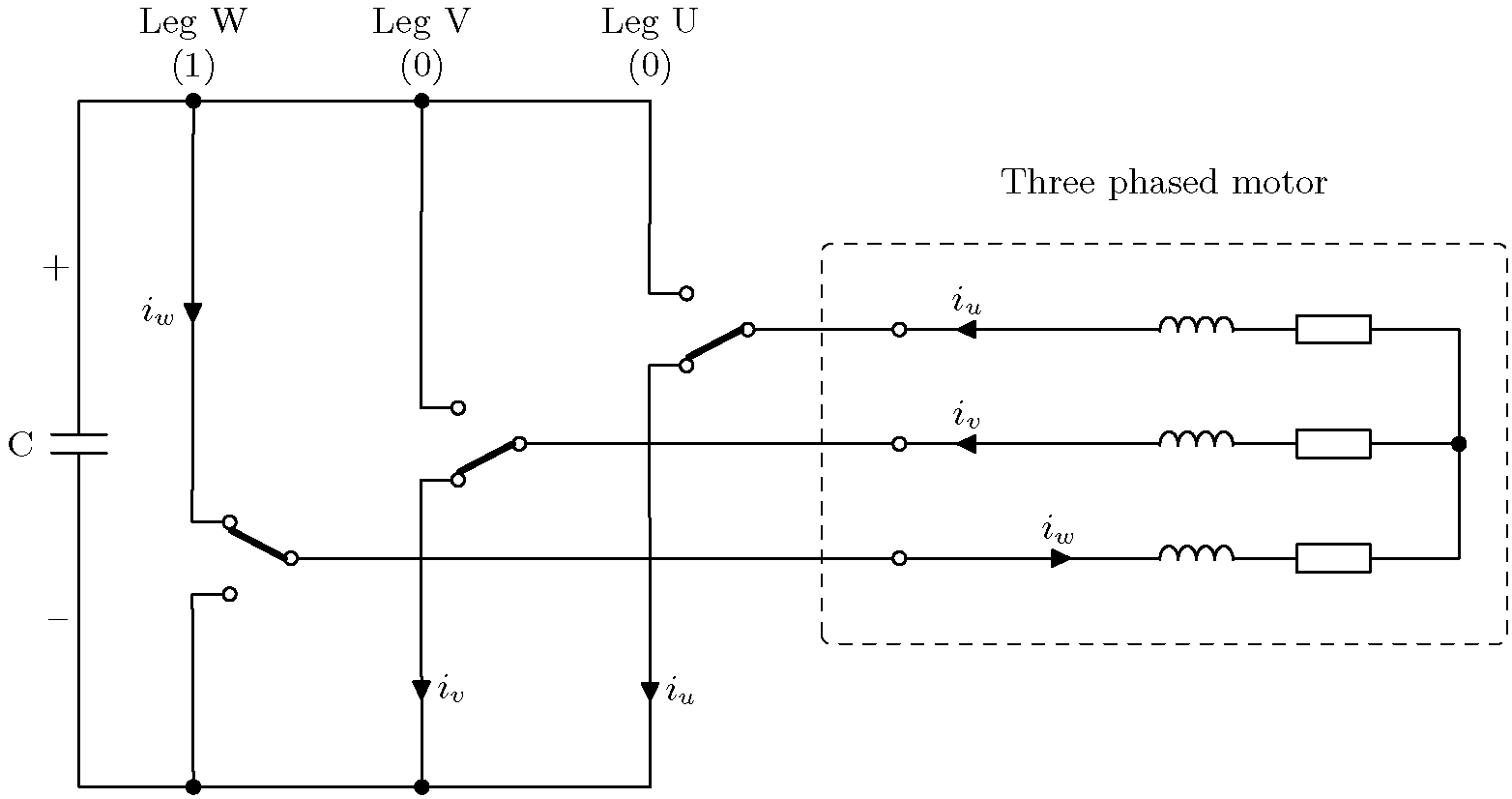
The simplified version of a two level inverter. The DC-link is now assumed constant so that the diode rectifier is omitted. Further, it is assumed that each inverter leg has one of two transistors closed at any given time. In this example, Leg W has the upper transistor closed while Leg V and U has the lower transistor closed. The arrows indicate current direction.
The above example shows a transistor combination where the leftmost leg (W) has its upper transistor closed and bottom transistor open. The two other legs (V and U) has its upper transistor open and lower transistor closed. This will correspond to a positive voltage being applied to W-phase while the two other phases are negative. The current arrows illustrate the current path from the positive DC link to the negative DC link.
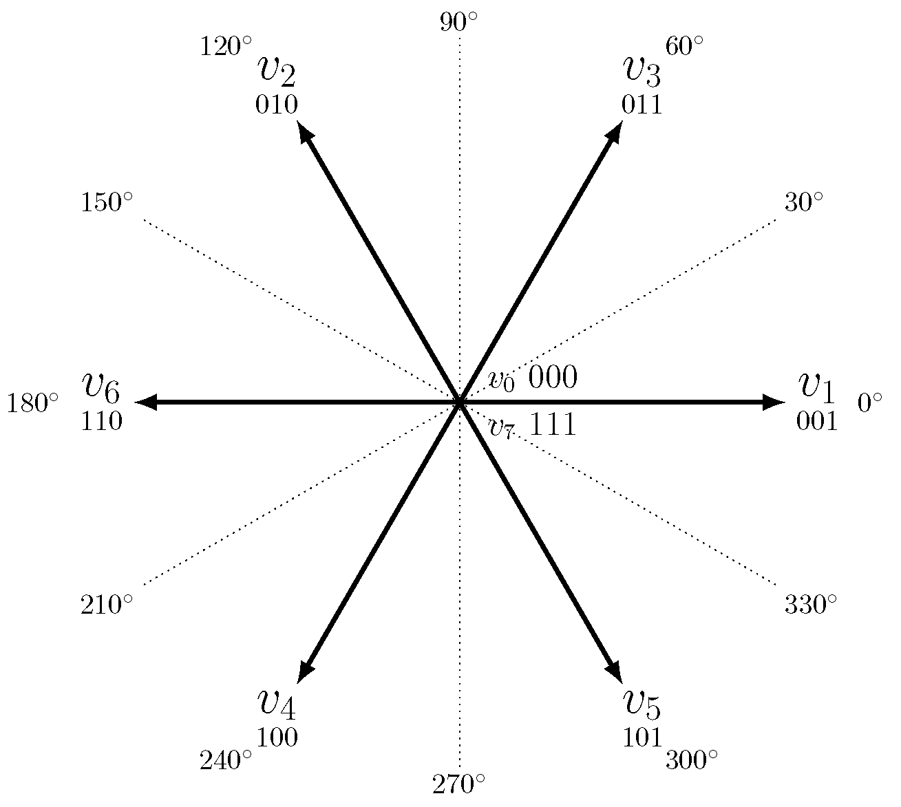
The eight basic vectors with their magnitude and direction. The zero vectors \(v_0\) and \(v_7\) are shown at origo. The U-phase is normally basis for all angles. The origin of the angles are the windings physical location inside the stator; installed around the circumference at 120° apart. Because each winding can have positive and negative voltage, it occupies two angles at 180° separation.
From the simplified schematic, it is now seen that there are three switches which can be in two different positions each. The total number of possible switch configuration is thus \(2^3 = 8\).
Six of these configurations correspond to different voltages applied to the connected motor and are called basic vectors from now on. The last two are referred to as zero vectors as they represent zero volts on the terminals.
The U-phase normally forms the basis for the basic vector's angles at 0°. The origin of the angles are the windings physical location inside the stator; installed around the circumference at 120° apart. Because each winding can have positive and negative voltage, it occupies two angles at 180° separation, e.g. 240° and 60° is W-phase in positive and negative state respectively.
In binary, these vector combinations can be represented as eight different binary values, here named from \(v_0\) to \(v_7\):
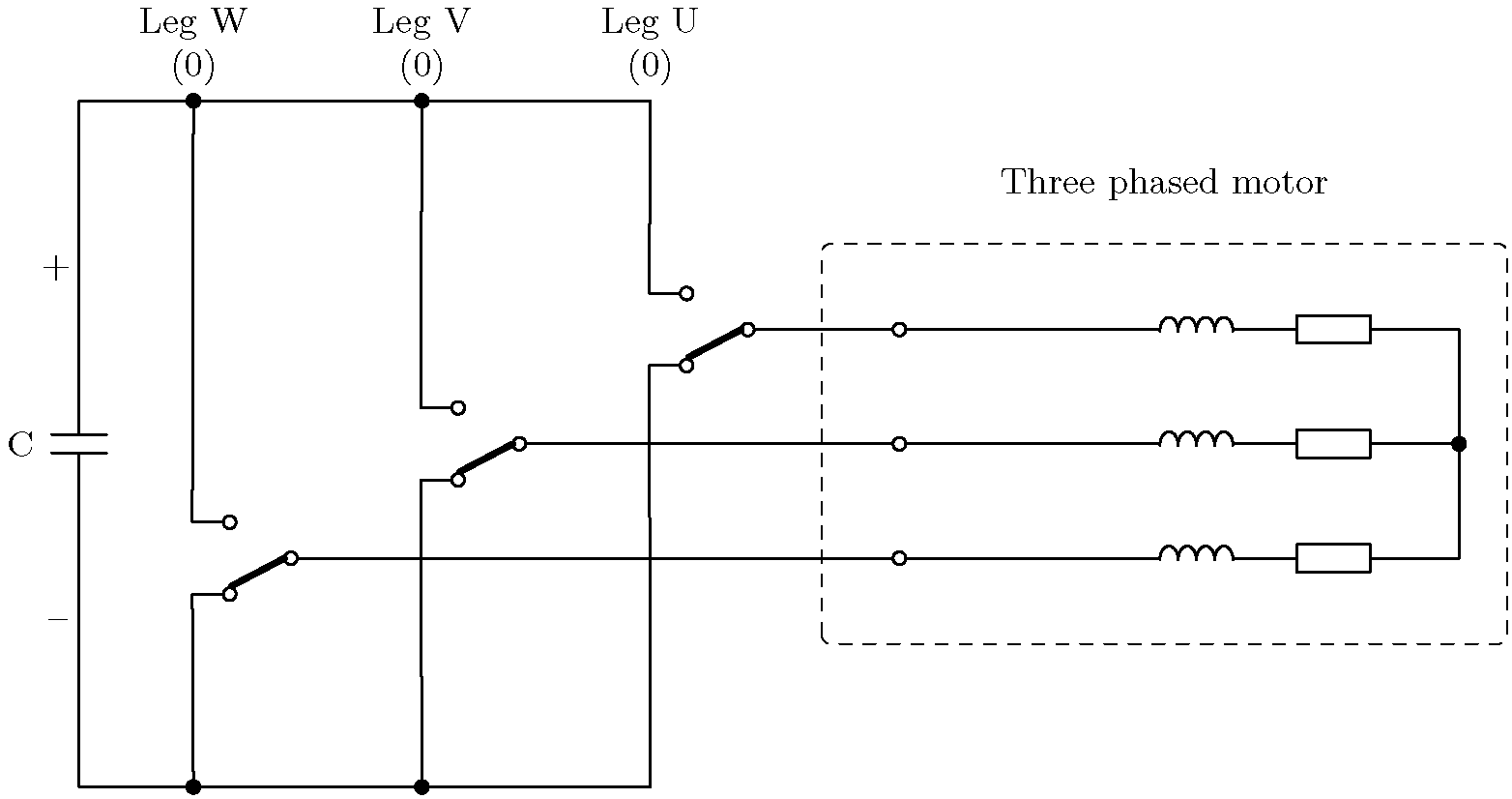
000 - \(v_0\) (zero vector)
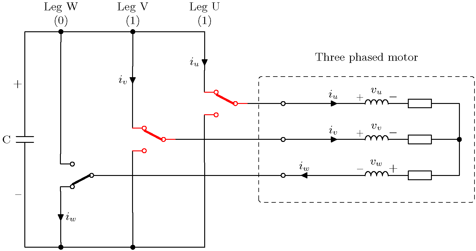
001 - \(v_1\) (Phase +U)
010 - \(v_2\) (Phase +V)
011 - \(v_3\) (Phase -W)
100 - \(v_4\) (Phase +W)
101 - \(v_5\) (Phase -V)
110 - \(v_6\) (Phase -U)
111 - \(v_7\) (zero vector)
Each of the three binary digits refers to one bridge leg where the value 1 indicates that the top transistor is closed whereas the value 0 indicates that the bottom transistor is closed.
All eight combinations and the resulting motor voltage and current directions are shown below.
Press any image to enlarge.
Synthesizing output voltage
So far it is only shown that the converter can output DC-link voltage to the terminals and how each of the six usable vectors affects current- and voltage directions in the motor.
A voltage reference between the basic vectors 1 and 3. Rapid alternations between these to vectors along with the zero vectors can emulate the reference voltage.
This section will show how to synthesize any voltage vector by quickly alternating between adjacent voltage vectors and timing of the on- and off times.
To the right there is an example of a reference vector which the inverter has to synthesize using the basic vectors available.
From the figure, it is seen that the reference is located between \(v_1\) and \(v_3\). This sector is called sector 1. It is now possible to quickly alternate between these two basic vectors to emulate a voltage vector at \(38.3^\circ\).
The two zero vectors \(v_0\) and \(v_7\) are also used to add dead time to the switching pattern. This dead time reduces the voltage magnitude and is necessary when the voltage reference magnitude is less then 100%.
The actual synthesizing can be achieved using a triangular wave as trigger. First is it assumed that the desired voltage reference is already available, e.g calculated by the reverse Clarke/Park transformation described in the Vector Control for Dummies post.
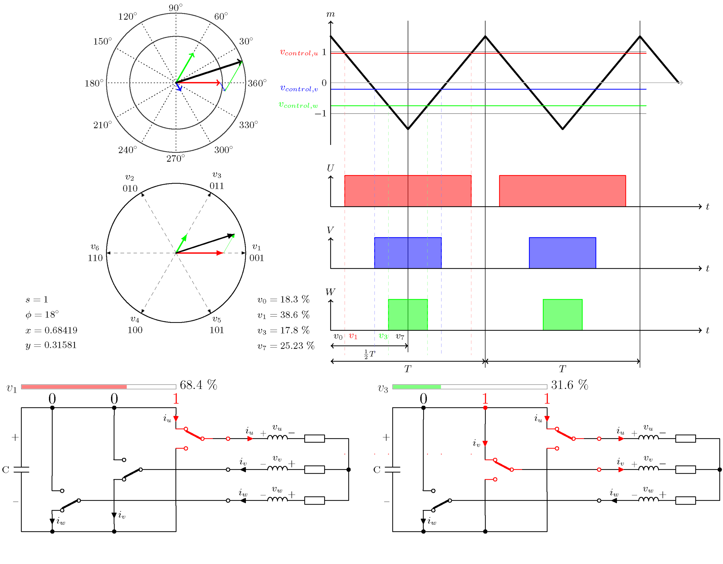
The figures below illustrate how a desired voltage is transformed into binary on/off signals for each of the three inverter legs by means of the triangular wave. Six different examples are shown, each with a different angle in different sectors.
Concept explanation
Let us take a breathing pause there. This figure contains a lot of information, and to better explain different parts of it, I have clipped out four different regions of it that will be explained below.
Part 1 - Input and projection to the trig wave:
Part 1 - The input which shows the desired output voltage and a trig wave used to determine the vectors used and their on-time.
The left circle is the "input" or "reference". Some also call it the order signal. It is what we want to achieve; three different voltages at different angles - together forming a space vector with one magnitude and one angle.
As seen, the U-phase (red) is close to its maximum positive value. This level is also shown on the graph to the right of the circle together with a triangle wave where it is referred to as a control voltage. The frequency of this waveform is many times higher than the frequency of the space vector. Typically between 1 and 20 kHz, but applications with a few hundred or hertz or up to hundreds of kilohertz are not unheard of.
The W-phase (green) is close to its maximum negative value and the V-phase (blue) just stretching out from zero in positive direction.
How these three values are intersected with the triangular wave will directly translate to which switches we want to close and how long we are keeping them closed.
Part 2 - Translating input to switching states:
Part 2 - The trig wave and how it visually translates into three binary digits. Here, 000-001-011-111 in the four different sections of the halv period.
Look at the right part of the figure.
The main focus in this part are the dashed lines protruding downwards from the triangular wave. These originate from where the control voltages intersect the trig wave. At all times, four different sections are visible below the W-axis right above the \(\frac{1}{2}T\) arrow. For other space vector angles and magnitudes, the width of these four sections change, but the total width will always be the same.
At the angle in this example (46°), the first dashed line is the red one. Between the start of the three axes and the red line, there are no active voltage vectors. All three control voltages in this region are below the trig wave. This means that all switches are off. 000. Zero vector \(v_0\).
Next section; between the red and the blue dashed line. The U-phase control voltage is now above the trig line while the two others are still below. This activates the U-switch. 001 there. Also called \(v_1\).
Third section: between the blue and the green line. Now both U and V is activated; 011 - \(v_3\).
Last section: All three switches are now active. This is 111, \(v_7\), the second zero vector.
At every angle and magnitude, the same pattern will be seen; Zero vector - basic vector - basic vector - zero vector. Repeat. The only thing that change is the width (i.e. the on-time) of these sectors and which of the six basic vectors are used.
Note that the on-time percentage is also displayed to the left of the W-axis. When the desired amplitude is low, the zero vectors will have an increased on-time and opposite when the amplitude is high. This is controlled by a scaling factor called modulation index. If the desired amplitude is higher than the trig wave, something called over modulation occurs. This is explained later.
Part 3 - Illustrating the vectors
Now we know that the two vectors we have to alternate between is \(v_1\) and \(v_3\).
By getting the on-times correctly, this will emulate a voltage vector at the same angle as the input voltage space vector.
You can see that the green \(v_3\)-vector is close to maximum both in the circle vector diagram and in the "sector diagram" below the W-axis. The same can be seen for the \(v_1\)-vector which is close to its minimum.
The thin line green line inside the space vector circle are visual aides to illustrate that these two basic vectors do indeed form the desired space vector as a vector sum.
The values to the left in the figure shows the angle, which sector we are in and the weighing factors, \(x\) and \(y\), for each of the two basic vectors. We will get back to those later.
Part 4 - Illustration of the two alternating switching configurations
The two different switching combinations (basic vectors) which the drive will alternate between is shown here. The progress bar above each configuration indicates how long it is on compared to the total on-time for both basic vectors. I.e, how long they are on relative to each other.
The zero-vectors come in addition and will increase for lower voltage levels.
Pay attention to that they are in opposite "phase" to each other, just as two sine waves 90 degrees apart. When the left configuration has completed its cycle, the right configuration is halfway.
This switching scheme also employs a nifty feature; only one switch is changing state at the time. This reduce harmonics in the machine and also reduces switching losses, a very important aspect to consider when designing any type of power electronics.
Summary
The by far most important part of the figure is the area below the lowest axis (W). It shows the portion each basic vector is active for each period \(T\). The percentage number is presented to the left of that axis.
It can also be seen that every pattern starts and ends with a zero vector, and that between every transition, only one switch is being changed. This greatly reduces harmonics in the motor which cause overheating and torque fluctuations. Also, any current that is not contributing to torque, or is necessary to maintain the required magnetic field, is unwanted. This is because the losses in the power electronic components are current dependent and they translate to heat which will stress the cooling system. Over-heating of transistors and diodes are one of the main challenges when designing power electronics today. The alternative is to design a converter with higher current ratings, but this increases the price.
Further, at the bottom of the above figure two schematics are shown. These represent the state of the switches for the two basic vectors which are in use in the current section. The percentage indication above indicate their on-time relative to the other. For example, if the angle is exactly between to basic vectors (i.e. 30°), both basic vector would be turned on 50% of the time each. Please note that this percentage does not indicate their total on time with respect to the period \(T\). If the voltage magnitude is less than maximum, there is added zero-vectors to averange down the voltage. So at 70% voltage magnitude and still at 30°, the ON-time of each basic vector is still 50% with respect to each other, but in total there would be 30% zero vectoring within this period. The actual on-time for each transistor thus become 35%;
\begin{equation}
T = T_{v_1} + T_{v_3} + T_{v_0} + T_{v_7} = 35\% + 35\% + 15\% + 15\% = 100\%
\end{equation}
A full animation is shown below.
Detailed example
Problem:
The drive has estimated that it needs to modulate a voltage vector of 630 V at an angle of 38.3°:
\begin{equation}
\vec{v}_s^u=630\angle38.3^\circ
\end{equation}
where the subscript \(s\) denotes a stator frame reference (i.e., not rotor) and the superscript \(u\) denotes that the angle reference (0°) is at phase U (0°) .
38.3° lies between basic vector 1 (0°) and 3 (60°), so these are the two we are going to utilize.
The equation to determine how much we are using each basic vector can be written as
\begin{equation}
\vec{v}_s^u = \hat{V}_s \angle \theta_{v_s} = x \cdot v_3 + y \cdot v_1
\end{equation}
where \(x\) and \(y\) are the unknown weighting factors for each vector and \(v_1\) and \(v_3\) are the two basic vectors in use.
The DC link voltage is 975 V and the motor nominal terminal voltage is 690 V (typical values in the marine industry)
First, the real component is established:
\begin{equation}
\mathfrak{R} \{\vec{v}_s^u\}
= \mathfrak{R}\{630\angle 38.3^\circ \}
= \mathfrak{R}\{x \cdot 975 \angle 60^\circ + y \cdot 975 \angle 0^\circ \}
\end{equation}
\begin{equation}
630\angle38.3^\circ = x \cdot 975 \cos{60^\circ} + y \cdot 975 \cos{0^\circ}
\end{equation}
\begin{equation}
630 \cdot 0.7848 = x \cdot 975 \cdot 0.5 + y \cdot 975 \cdot 1
\end{equation}
\begin{equation}
\label{eq:x}
494.409 = x \cdot 487.50 + y \cdot 975
\end{equation}
Secondly, we establish the imaginary component:
\begin{equation}
\mathfrak{I} \{\vec{v}_s^u\}
= \mathfrak{I} \{630\angle 38.3^\circ \}
= \mathfrak{I}\{x \cdot 975 \angle 60^\circ + y \cdot 975 \angle 0^\circ \}
\end{equation}
\begin{equation}
630\angle38.3^\circ = x \cdot 975 \sin{60^\circ} + y \cdot 975 \sin{0^\circ}
\end{equation}
\begin{equation}
630 \cdot 0.6198 = x \cdot 975 \cdot \frac{\sqrt{3}}{2} + y \cdot 975 \cdot 0
\end{equation}
\begin{equation}
\label{eq:y}
390.461 = x \cdot 844.37 + 0
\end{equation}
We can now find \(x\) and \(y\) by setting up equation \ref{eq:x} and \ref{eq:y} towards each other:
\begin{equation}
390.461 = x \cdot 844.37 + 0
\end{equation}
\begin{equation}
x=\frac{390.461}{844.37} = 0.4624
\end{equation}
Inserting the \(x\)-value into the equation for \(y\):
\begin{equation}
494.409 = x \cdot 487.50 + y \cdot 975
\end{equation}
\begin{equation}
494.409 = 0.4624 \cdot 487.50 + y \cdot 975
\end{equation}
\begin{equation}
y=\frac{494.409-(0.4624 \cdot 487.50)}{975} = 0.2759
\end{equation}
Let us double-check the result by inserting the values we have found:
\begin{equation}
\vec{v}_s^u
= \hat{V}_s \angle \theta_{v_s}
= x \cdot v_3 + y \cdot v_1
= 0.4624 \cdot 975 \angle 60^\circ + 0.2759 \cdot 975 \angle 0^\circ = 629.999\angle38.297^\circ
\end{equation}
This result is pretty close to the original target, which was 630 V at an angle of 38.3°
So what will the output voltage be?
The available voltage at the inverter terminals are not readily apparent by looking at the schematics alone due to the averaging of different vectors and the use of a modulation index.
Let us start at the beginning and see where we end up:
The grid voltage which the rectifier is connected to:
\begin{equation}
V_{grid, RMS} = 690 V_{RMS}
\end{equation}
The resulting DC-link voltage (assumed low load):
\begin{equation}
V_{DC} = V_{grid, RMS} \times \sqrt{2} = 975.8 V
\end{equation}
Alternative formula DC-link voltage (average for three phase / six pulse supply):
\begin{equation}
\cfrac{3\sqrt{2}V_{RMS}}{\pi} = 931 V
\end{equation}
(for now we will stick with the first one, and get back to the last one later)
This voltage level is what we have to play with to synthesize an output voltage.
The famous space vector hexagon showing each of the basic vectors and their magnitudes along with a reference vector at 30° which has a maximum linear magnitude.
As shown earlier, there are six basic vectors, but their magnitude has not been stated yet — only their angles. So here goes:
\begin{equation}
\left|v_{1-6}\right| = V_{DC}
\end{equation}
Tada. That wasn't so difficult?
With the above information an updated figure of the six basic vectors can be presented. When lines are drawn between each vector tip, it will form the well known space vector hexagon. Note that in the literature, different notation for the space vector hexagon are used; phase voltage, line voltage, RMS voltage and some include over modulation as well (we'll get to that, don't worry).
The observant reader might notice a circle located inside the hexagon. Its radius is given by the maximum size permissible by the boundaries of the hexagon. This radius is given at \(30^{\circ}\) which is exactly between two adjacent basic vectors.
The maximum RMS output voltage then becomes:
\begin{equation}
V_{max,RMS} = V_{DC} \times \cos{30^{\circ}} \times \frac{1}{\sqrt{2}} = 597 V
\end{equation}
This is lower than the input voltage, but the reason for this is apparent when looking at the hexagon; when alternating between to adjacent basic vectors, we are averaging and in the process some of the voltage is "lost".
This low voltage might come to some as a slight disappointment. When your grid voltage is 690 V, you would want to buy a 690 V motor to go with it.
What do we do now?
Third harmonic injection
Fasten your seat belts and whip out your wand, because we are now heading towards the dark arts of electrical engineering.
As just shown, we are faced with a challenge with too low output voltage compared to what we really want. But we are also faced with physical limitations. Which we are going to bend. Slightly.
First, let us illustrate the problem below:
A standard two-level inverter shown with its maximum output voltage waveform in red. The dashed curve represent the desired voltage, i.e. same amplitude as the input rms voltage.
The maximum voltage output of the DC-link has to be the DC-link voltage. Above it is shown as a red sine wave where the peak-to-peak voltage equals \(V_{DC} = 975 V\). The RMS phase-to-phase voltage then becomes:
\begin{equation}
V_{max,RMS} = \frac{V_{DC}}{2} \times \sqrt{3} \times \frac{1}{\sqrt{2}} = 597 V
\end{equation}
which is exactly the same as we just stated a few paragraphs up, just presented from a different perspective. And we still haven't touched our problem besides illustrating that we need to go through the DC-link ceiling somehow by approximately 15% to reach 690 V. This might seem impossible; The ceiling represent a switching state where the switches are on 100% of the time, while the floor represent a zero on-time. So how can a switch be on more than 100% or less than 0% ?
The trick we need to pull was invented by an engineer working for GE in the 1980s and is called (fanfare); Third Harmonic Injection.
That's right folks; Adding a second sine wave with a frequency three times the fundamental frequency will effectively solve our problem in a very elegant way as shown below:
Third harmonic injection; hidden inside the blue waveform is a fundamental sine wave with amplitude above the DC-link voltage.
Wait, you say? Did some pay for a smooth sine wave?
Well, the trick is that it's all hidden inside. By expanding the blue curve above to its constituent sine waves (a.k.a Fourier expansion), the following will appear:
The third and fundamental harmonic exposed, revealing the increased amplitude.
Three phases with their first and third harmonics. Note that the third harmonic (black) is common to all three phases.
Now that is more like it! We have now successfully circumvented physical limitations in terms of maximum voltage output and packed it all neatly with the use of third harmonic injection.
Next we will look at what the motor thinks of this. Harmonics is almost always an unwanted phenomenon, so let's check the consequences.
The figure to the right illustrates all three phase voltages with third harmonic injection.
Some might notice something odd with those curves; The black third harmonic curve is common to all three phases. All three are super positioned and are totally identical which means that the third harmonic is now a common mode wave form. Now all parts of the motor circuit will oscillate at three times the frequency with respect to the DC-link.
A volt-meter connected to the phase-neutral points of a motor. This will reveal the motor winding voltage and if the third harmonics will have any effect on them.
The neutral point of the motor is now of particular interest. The question now becomes:
What is the phase-to-neutral voltage across each winding?
Recall that the phase voltage consist of a big sine wave and a third harmonic wave added together. The scope will now display the phase voltage (the left probe in the figure) minus the neutral voltage (the right probe).
Also remember that every point in the motor is oscillating at the third harmonic frequency and amplitude, including the neutral point. The neutral-connected probe will therefore also see the same third harmonic which is measurable at the phase-connected probe.
The mathematics then becomes something like this:
(Big sinewave + third harmonic sinewave) — (third harmonic sine wave) = (Only big sinewave)
Oh yeah. The whole third harmonic component goes away and the winding doesn't even know about it.
Bazinga.
Modulation index, m
This is quite simply a factor used to scale the voltage. In the last section it was shown that the output voltage can be scaled up to 115.4% by applying third harmonic injections. I.e. the modulation index can span from 0 to 1.154
The formula for output phase-to-phase voltage then becomes
\begin{equation}
V_{max,RMS} = \frac{V_{DC}}{2} \times \sqrt{3} \times \frac{1}{\sqrt{2}} \times m
\end{equation}
where \(m\) represent the modulation index factor.
The below animation illustrates the concept:
The voltages as function of modulation index m. A smooth sine wave can be synthesized with 0 < m < 1.154 by use of third harmonic injection.
Over modulation
For modulation index beyond 1.154 strange things will start to happen. The control voltages used in conjunction with the triangular wave will move above the trig wave. This will effectively remove zero vectors and depending on how far above the control voltage moves, it will also dominate the other control voltages for longer and longer periods within each own sector.
The inverter will cut pulses and distort (roughen up) the sinusoidal wave more and more until a situation called six step occurs. In six step operation, the inverter will stay at one basic vector at the time and jump directly to the next basic vector and then to the next and so forth. With 60 degree steps and square wave operation, the motor will produce a lot for harmonics and probably feel really terrible. Luckily, the motor inductance will filter (smoothen) the current to avoid damage due to exessive cogging / torque ripple (remember, it is the current that produces the torque - not the voltage).
This mode of operation is exactly what we tried to avoid initially by doing our averging of two different and adjacent basic vectors.
Even though over modulation seems like motor torture (which it is...), it is sometimes necessary. Up till now it has been assumed that the DC-link always stays at a factor of \(\sqrt{2}\) above the supply voltage, but that is not always the case.
When high currents are needed, such as when the motor is running at full speed and full power, the current drawn from the grid is substantial, causing the small DC resistance in the rectifier diodes to become huge voltage drops (Ohm's law there, folks).
Suddenly the DC-link voltage is no longer 975 V, but 900 V and at full speed the motor requires full voltage in order to keep the motor flux at rated value. At this voltage, a modulation index of 1.25 is required, and this will create an ugly sine wave. Also, note that over-modulation is no longer linear. It actually looks more like the saturation region of a magnetizing curve, meaning that the controller will have to amplify the modulation index in order to achieve the desired (linearized) modulation level.
Due to the ugly sine wave, harmonics other than our designed third harmonic start to appear. These can cause over heating of both rotor and main windings along with acoustic noise (whining) and torque ripples. Note that this applies to induction motors. Brushless DC-machines are actually designed for this mode of operation


